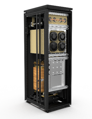
A major milestone for the FOR²ENSiCS project has been reached with the development of a 10 kV DC/DC transformer prototype
After two and a half years of dedicated research and innovation, the FOR²ENSiCS project has reached a major milestone: the successful development of a 10 kV DC/DC transformer prototype! This achievement represents an important step forward in the advancement of high-voltage, high-efficiency power conversion technologies! The prototype has now been installed on our technology testing platform at SuperGrid Institute where it will undergo testing over the coming year.
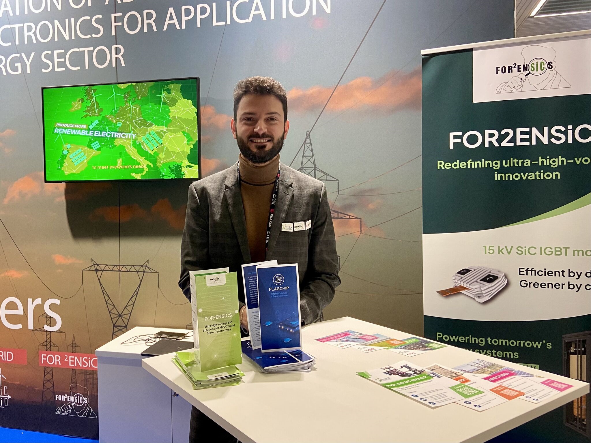
The FOR²ENSiCS project aims to develop disruptive ultra-high-voltage (UHV) SiC materials and devices, paving the way for more compact, efficient and reliable power electronics with significantly reduced losses and carbon emissions. Unlike the current industry roadmap, FOR²ENSiCS targets bipolar SiC devices above 10 kV, creating new opportunities for grid applications.
A prototype featuring several breakthrough technology building blocks
The newly developed DC/DC transformer prototype integrates multiple cutting-edge components, including:
- Europe’s first 15 kV Silicon Carbide (SiC) IGBT device
- An advanced high-voltage module architecture
- A 10 kHz Medium-Frequency Transformer (MFT)
- A series-connected SiC MOSFET switch
This prototype serves as a versatile testbed for both low- and medium-voltage inverters, as well as medium-frequency transformers. It plays a key role in enabling a substantial reduction in weight, size and material usage compared to conventional 50 Hz transformers. This is one of the primary objectives of the FOR²ENSiCS initiative.
An advanced module architecture has been developed to support the integration of the 15 kV SiC IGBT. This architecture can withstand high voltages while ensuring efficient thermal management of the SiC chips, addressing one of the major challenges in high-voltage power electronics.
The DC/DC solid-state transformer has been specifically designed to meet the evolving needs of emerging Medium-Voltage DC (MVDC) networks. Thanks to Its high modularity and versatility, it is well-suited to a broad range of future applications in energy distribution and electrification.
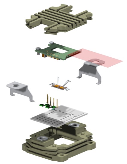

The 15 kV SiC IGBT
Looking ahead: a year of validation and reliability testing
As the FOR²ENSiCS project enters its final year, the focus will be on extensive testing of the demonstrator and on validating the reliability of each individual component. These upcoming activities will be crucial to ensure the robustness, performance and long-term viability of the technologies developed throughout the project.
November highlights: FOR²ENSiCS takes the spotlight
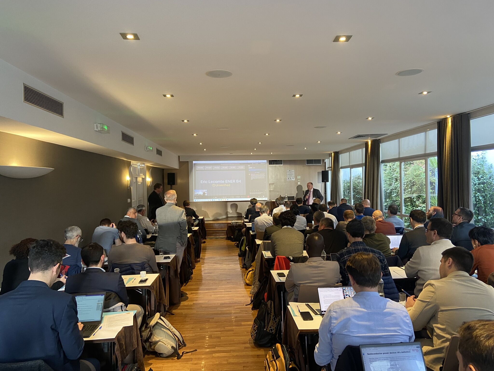
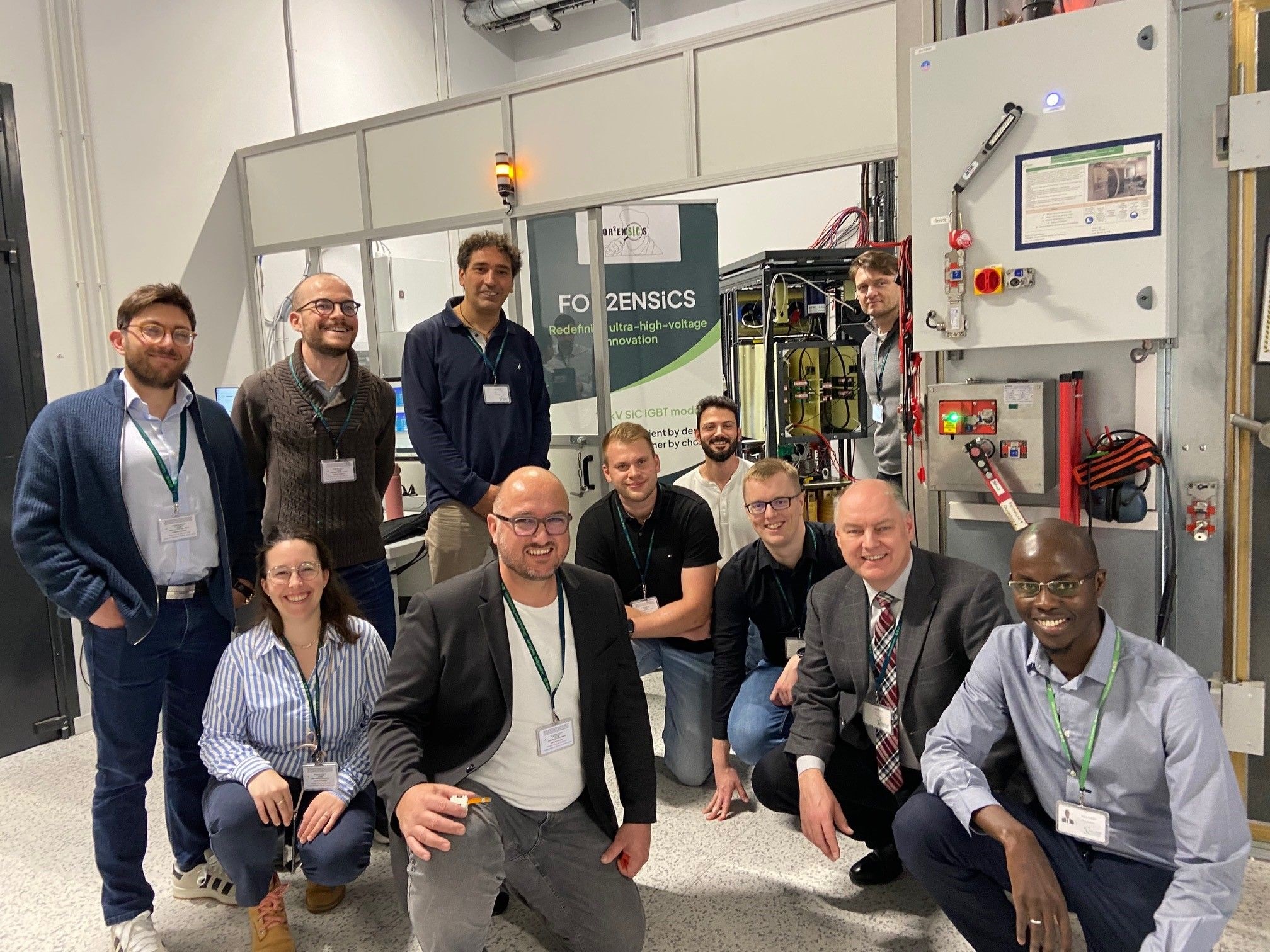
The FOR²ENSiCS prototype was recently showcased during the ECPE Workshop on Ultra-High-Voltage Power Electronics, held in Lyon on the 12th of November. On this occasion, Besar ASLLANI, project leader at SuperGrid Institute, guided a group of international experts through a dedicated lab tour, offering them a firsthand look at the newly developed 10 kV DC/DC transformer prototype.
During the visit, participants discovered the technical advances achieved within FOR²ENSiCS, with live demonstrations delivered by our engineering teams and consortium members. The event sparked rich discussions on SiC technologies, grid integration and the future of high-voltage power conversion.
“The workshop confirmed that ultra-high-voltage SiC technologies will play a central role in future MVDC networks. Through FOR²ENSiCS, we are contributing key building blocks to this transition, and it was a privilege to discuss these advancements directly with industry and research players.”
The visit highlighted the importance of collaborative research in accelerating innovation in ultra-high-voltage SiC devices and next-generation solid-state transformers. It also reinforced the visibility and impact of the FOR²ENSiCS project within the European research community.
“I was overwhelmed by the interest in the topic and the renowned speakers volunteering to become part of the programme. After all, it became an exchange on an astonishingly high level. The workshop was complemented by an inspiring visit to the SuperGrid Institute. We saw the latest developments and – even more important – we could discuss with the scientists. At least I left with a few good ideas.”
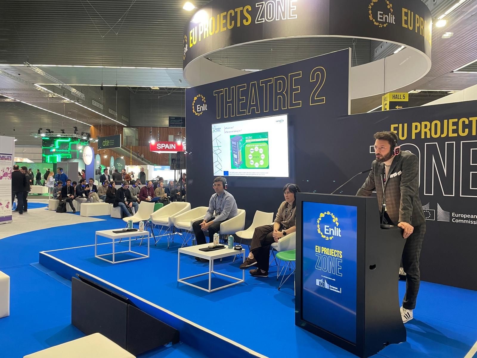
At Enlit Europe, Besar ASLLANI presented the objectives, technical approach and latest progress of FOR²ENSiCS during a dedicated session. This event offered a valuable opportunity to raise awareness of the project’s advancements and their significance for the development of future power electronic architectures.
“Enlit Europe offered a unique environment to present our work to a broader audience and to demonstrate how FOR²ENSiCS is contributing to next-generation high-voltage power conversion solutions,” added Besar ASLLANI.
These two events increased the visibility of FOR²ENSiCS and emphasises the collaborative momentum driving innovation in high-voltage SiC power electronics.
FOR²ENSiCS – Expected results
- Improved process for Ultra High Voltage SiC bipolar devices manufacturing with high yield
- Splitting process for reuse of SiC Wafer up to 10 times
- Development and manufacturing of 15 kV SiC IGBTs
- Development and manufacturing a 15 kV power module based on the 15 kV IGBT
- Increased reliability of 15 kV SiC IGTBs and 3.3 kV SiC MOSFETs
- Development and manufacturing 10 kV – 10 kHz – 250 kW Medium Frequency transformer
- Development and manufacturing 10 kV – 250 kW Inverter based on series connected 3.3 kV SiC MOSFETs
- Development and manufacturing of a 1.5 kV to 10 kV 250 kW DC/DC Solid State Transformer for MVDC applications
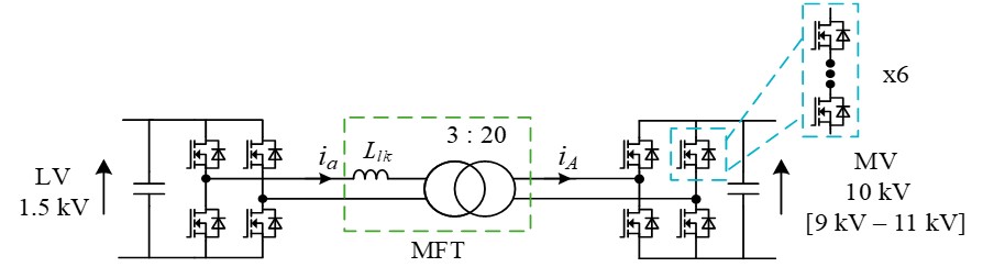
FOR²ENSiCS bidirectional MV DC/DC transformer
This project has received funding from fhe European Union’s Horizon Europe research and innovation programme under grant agreement No 101075672